| Home | Papers | Reports | Projects | Code Fragments | Dissertations | Presentations | Posters | Proposals | Lectures given | Course notes |
|
|
An analog 4 way stereo audio SplitterWerner Van Belle1* - werner@yellowcouch.org, werner.van.belle@gmail.com Abstract : We provide the schematics of a 4 way audiosplitter. It takes 1 stereo input and generates 4 stereo outputs. It has a volume knob that will go to 11 if need be.
Keywords:
|
Table Of Contents
| Circuit Design Prototype Transfer Function | PCB Design Calibrating the photo sensitive plate Removing copper Adding components Packaging Bibliography |
Circuit Design
Prototype
The design of the splitter is based on a simple audio opamp (NE5532A). The schematics are created after weeks of discussion with my brother (I'm no expert in audio circuit design), after bringing together various sources [1] and after testing whether various capacitance's and resistors 'sounded' OK.

|
The most tricky thing with that particular opamp is how to deal with negative voltages. In particular, the NE5532 assumes there will be a +5V and -5V present. Connecting ground and +Vcc to pin 4 and 8 respectively will not allow the opamp to generate a signal below 0V. To solve that, a biasing is introduced by adding a Vcc/2 reference voltage to the circuit. To generate that voltage we can resort a) to two resistors between +Vcc and ground. Although some people swear by this strategy, others claim it will not work. Another strategy is b) to use a second opamp to generate Vcc/2 (See [2]). Also with this solution some people claim it is the wrong tool for the job. Others swear by this strategy. In practice I tried them both and the solution with 2 parallel resistors works equally as good as the solution with a second opamp. If a load would be attached the middle output might indeed not be at Vcc/2. However, the opamp is no load. Secondly. The Vcc/2 line must just be larger than the input amplitude. Whether it is exactly Vcc/2 or not doesn't matter.
Once the biasing potential is created it has to be added to the chip, in such a way that the inputs and outputs are shielded from it. That is done by the coupling capacitors CIL, CIR and COL, COR. Everything between these two capacitors can have a dc offset, without affecting the input nor the outputs. The dc offset is added to the positive inputs of the opamp. This trick is taken from [3]
| ||||
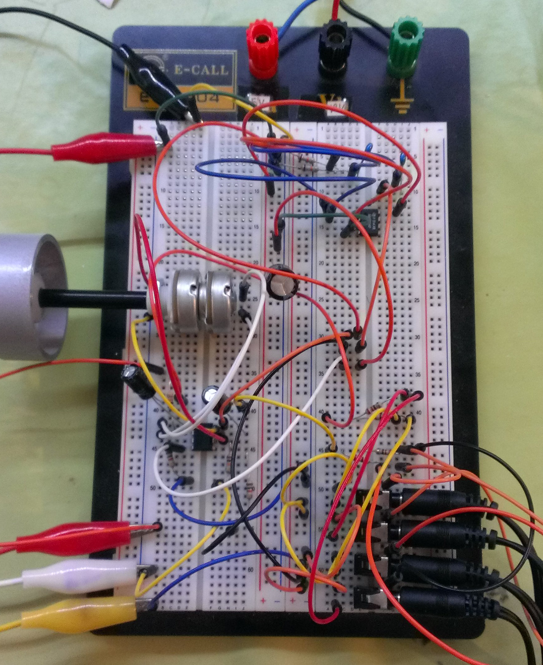
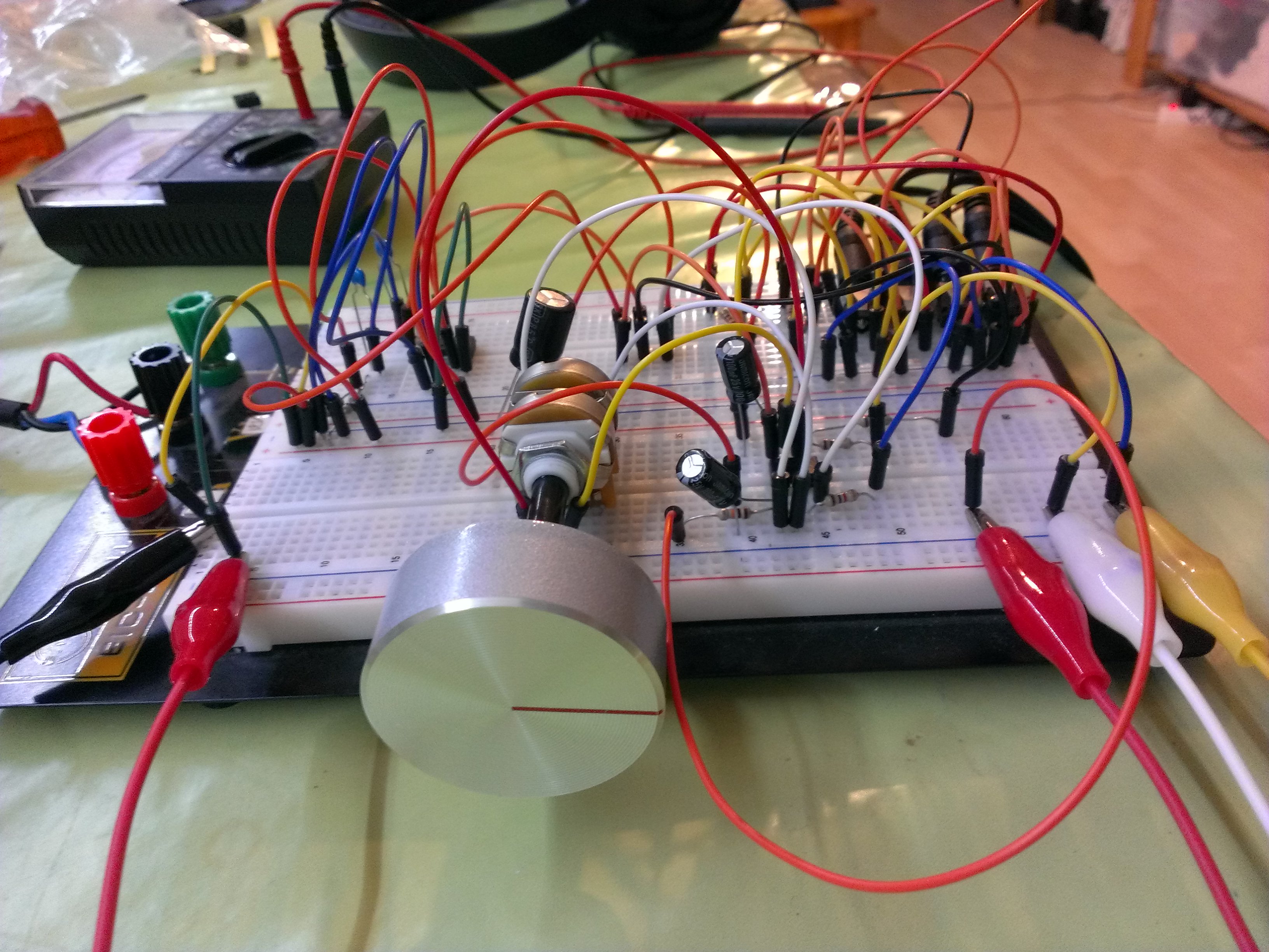
| Prototyping the audio splitter. This particular instance has the Vcc/2 opamp solution |
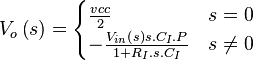
Transfer Function
To obtain the transferfunction [4], first calculate how Vo (the output of the opamp) relates to Vin. To do that we look at the negative input node of AMP1. The input currents into this node must all sum out to be zero. The first current comes over the input coupling capacitor (CIL for left. CIR for right. C_I in the equations) and the resistors (RSL/RSR. R_I in the equations).
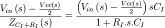
The second input current comes over the poti (with resistance P). It is
The sum of these both should be 0, thus
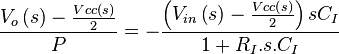
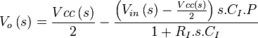
Because Vcc(s) is zero for all frequencies except 0, we have
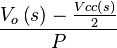
The output section from Vo to Vout, which is measured over H (headphone) is given by the current flowing from Vo to ground over the output coupling capacitor CO and H
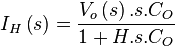
Vout is then
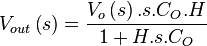
When s=0 we have Vout(0)=0. When s!=0, we have
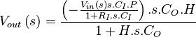
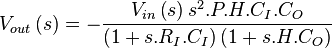
Dividing Vout by Vin and then inserting i.omega in s gives the transferfunction
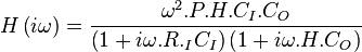
The headphone section has been modelled as an overall resistance H,
which depends on the impedance of the headphone, the resistor Ro, and
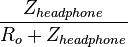
the number of headphones connected (n). We have 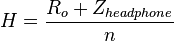 . The actual voltage over the headphone is
 . In our
case about 33%. Secondly. The power through each section is divided by
the number of headphones.
. In our
case about 33%. Secondly. The power through each section is divided by
the number of headphones.
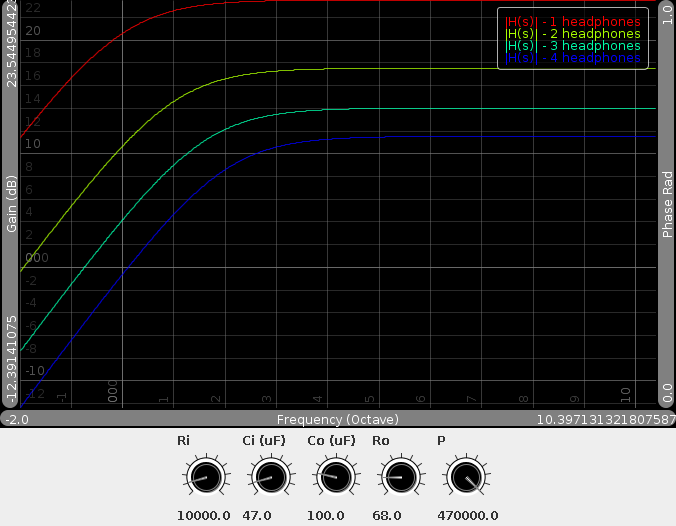 H(s) calculated with pot at max and n headhphones
|
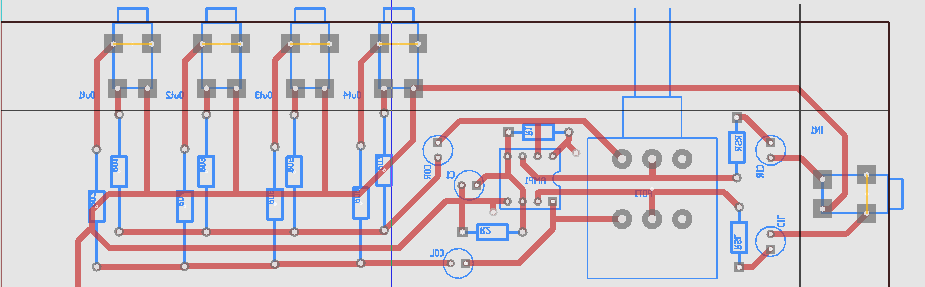
PCB
Design
The design of the PCB was slightly more complicated that I would have expected. Routing the various lines on a 2D surface was a surprising topological problem. In the end, a lot of manual work was involved to bring the inputs of the opamp as close as possible to the chip (See [5], section on PCB layout and how to avoid noise).
|
Calibrating the photo sensitive plate
| ||||
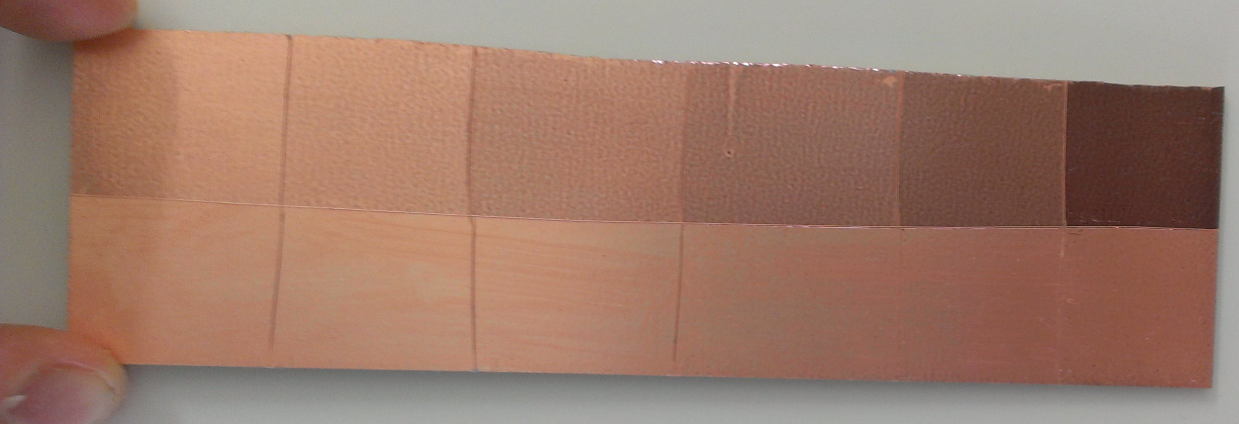
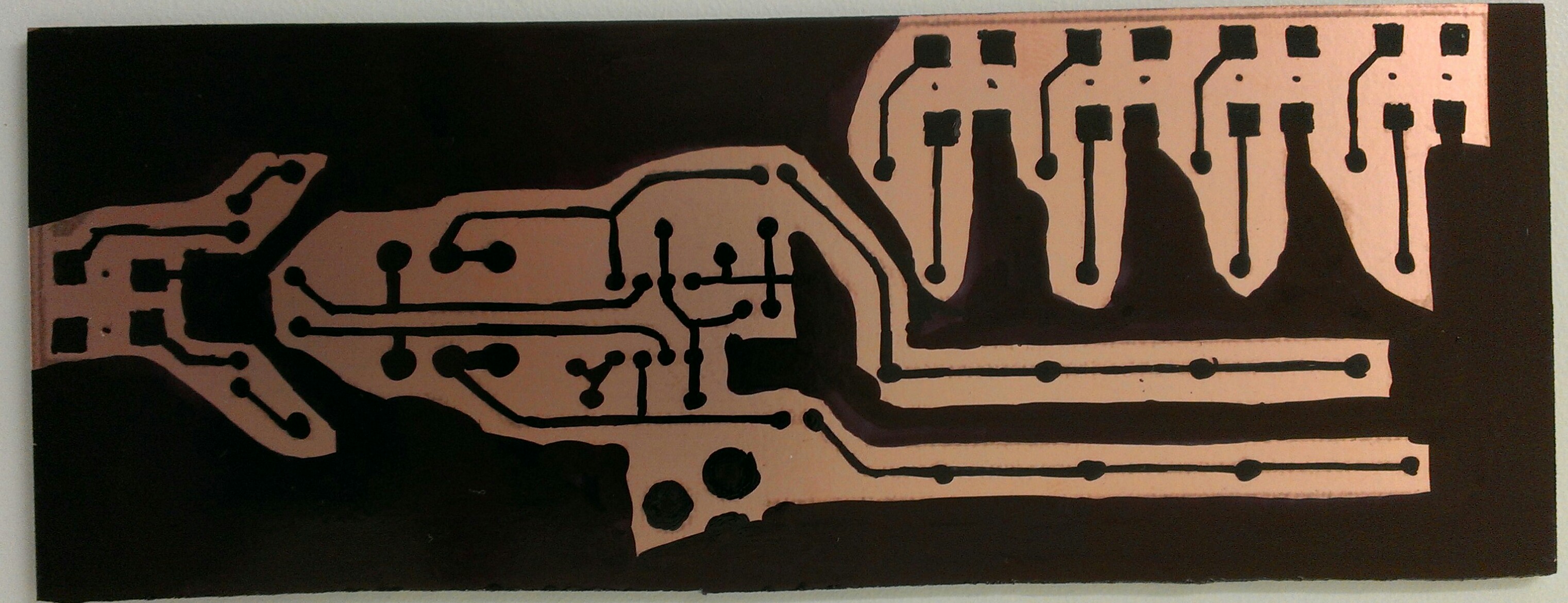
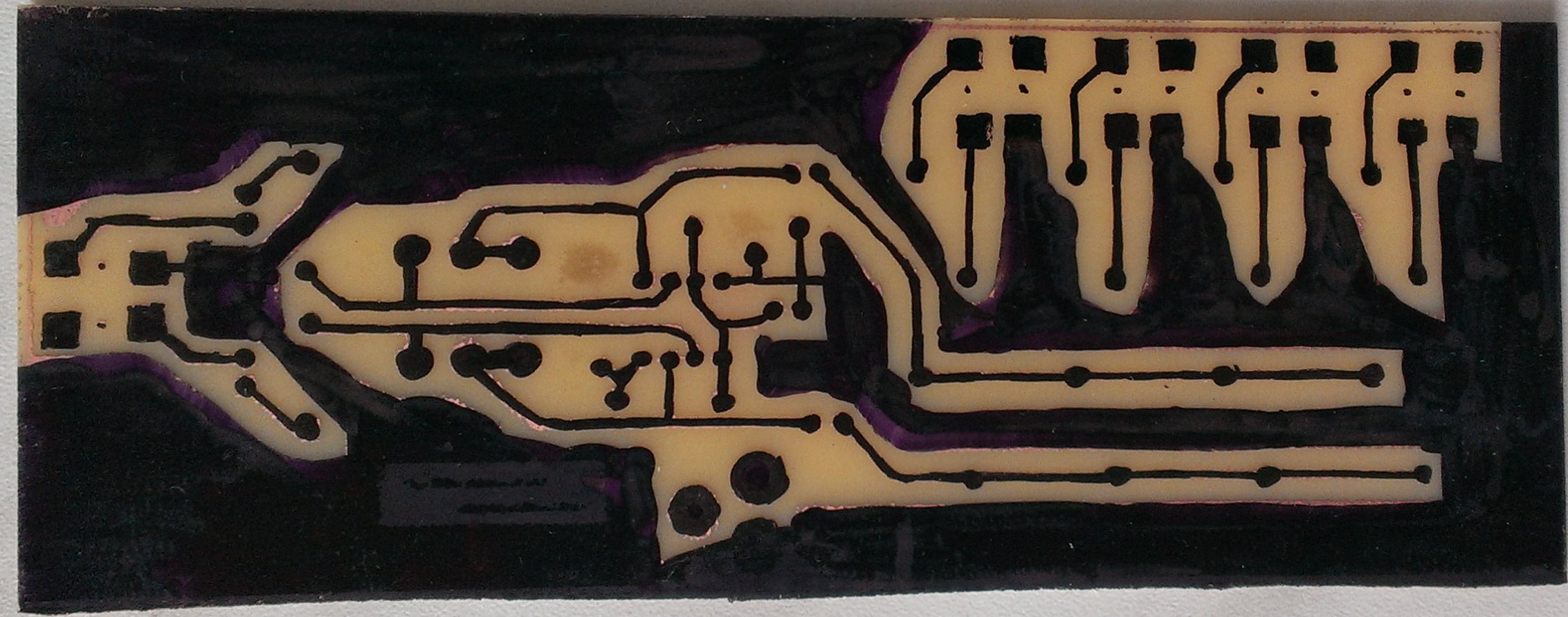
To print the PCB I relied on a guide by [6]. One of the first sections explains that a positive image should be imprinted on the PCB. This is done by printing out the layout on transparent slides. Then shining UV light on it. The areas that received UV will be removable by NaOH. The ones that stayed in the dark should -theoretically- stick to the plate. Now, I have a couple of intense UV-C tubes, and I have NaOH. Yet the appropriate duration and concentrations was not quite clear to me. To get a better grasp on that I followed the manual that accompanied the photosensitive plates. Every 20 seconds I opened up a new window. The results were not good. There was no level of light that would not remove the non-UV-exposed film. It might be possible that the NaOH solution was too strong, or the light was too strong, or the toner was insufficiently dark (allthough, I already layered two films). In any case, it didn't really work out the way it should. In the end, I used the photosensitive plate to make a print and then manually inked the copper that should not be removed.
Removing copper
| ||||
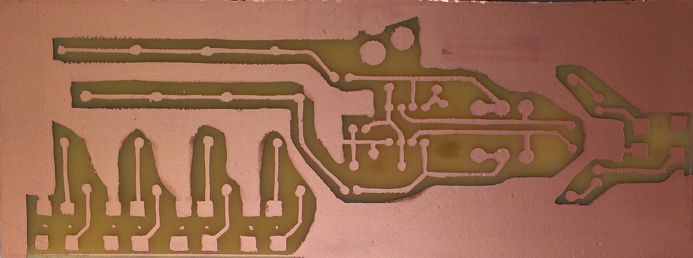
The next step is dissolving the copper film through chemical means. Ordinarily Fe(III)Cl3 is used for this purpose. Yet finding Iron-(III)-Chloride is apparently a tricky business now. With all those the-rho-rhists and so. Basically, you can't buy it anymore from Reichelt. Instead you have to buy natriumpersulfate, which oddly enough actually did the work and is a lot cleaner than that iron based solution we all got used to. Bottomline is that after agreeing that I would not use that persulfate to blow up shit and so; and stirring in a 55 degree bath for 10 minutes, we successfully eradicated the copper.
After that it was only a matter of removing the ink. Then a metal protection spray was used as suggested by [6].
Adding components
| ||||
| Adding components to the PCB |
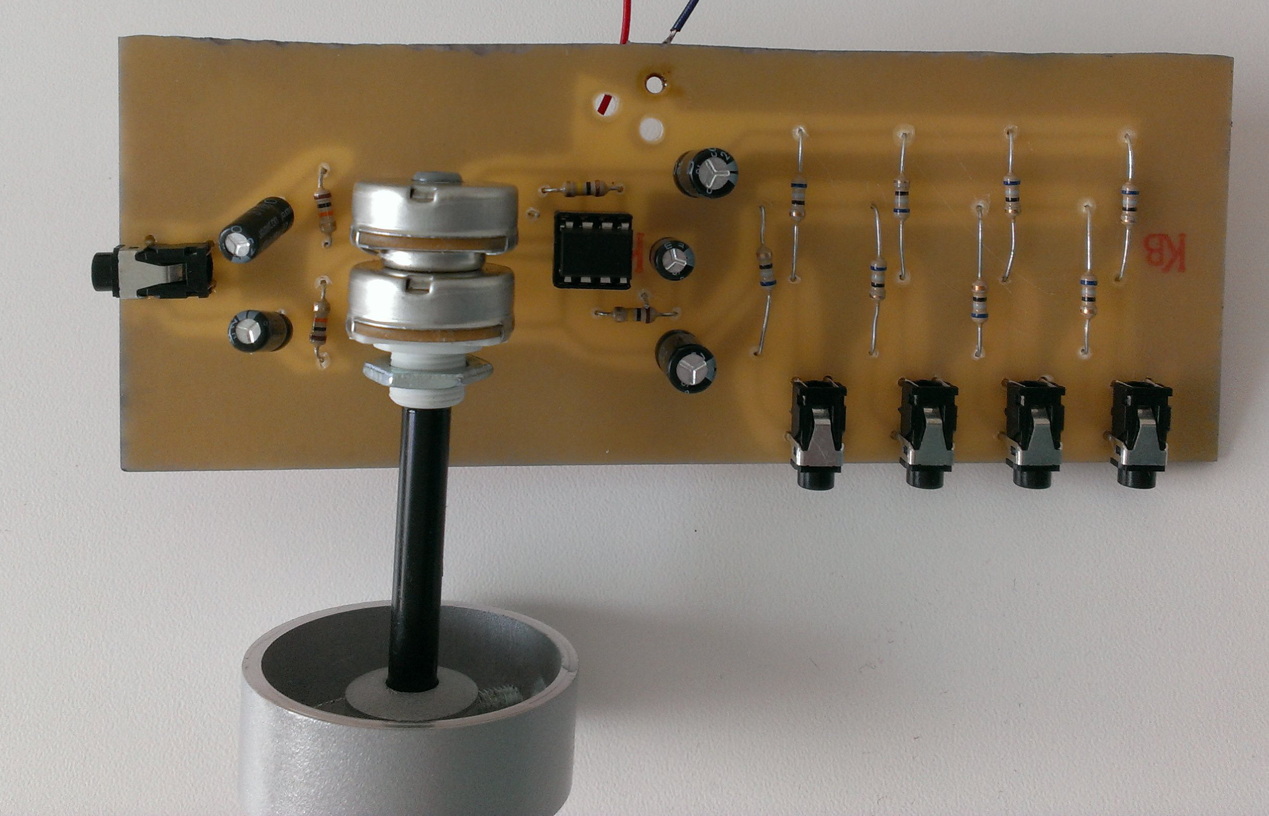
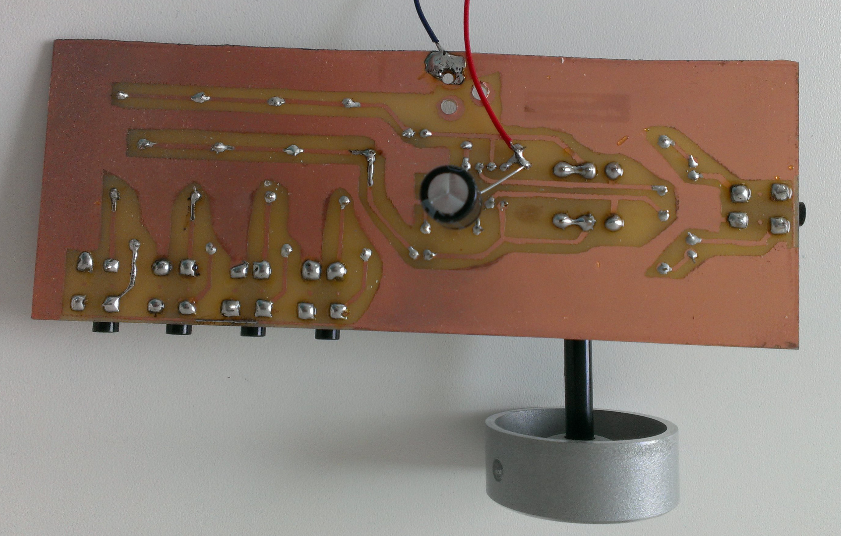
To add components, my wife and I cooperated (given that I am no good at fine work). I would do the solid 'bolted on' components, like power supply and jacks. She would do the more subtle work. One particular component we placed at an odd location: to simplify routing and reduce noise we placed the LPF capacitor across the chip, from pin 1 to pin 8, at the bottom of the plate.
Packaging
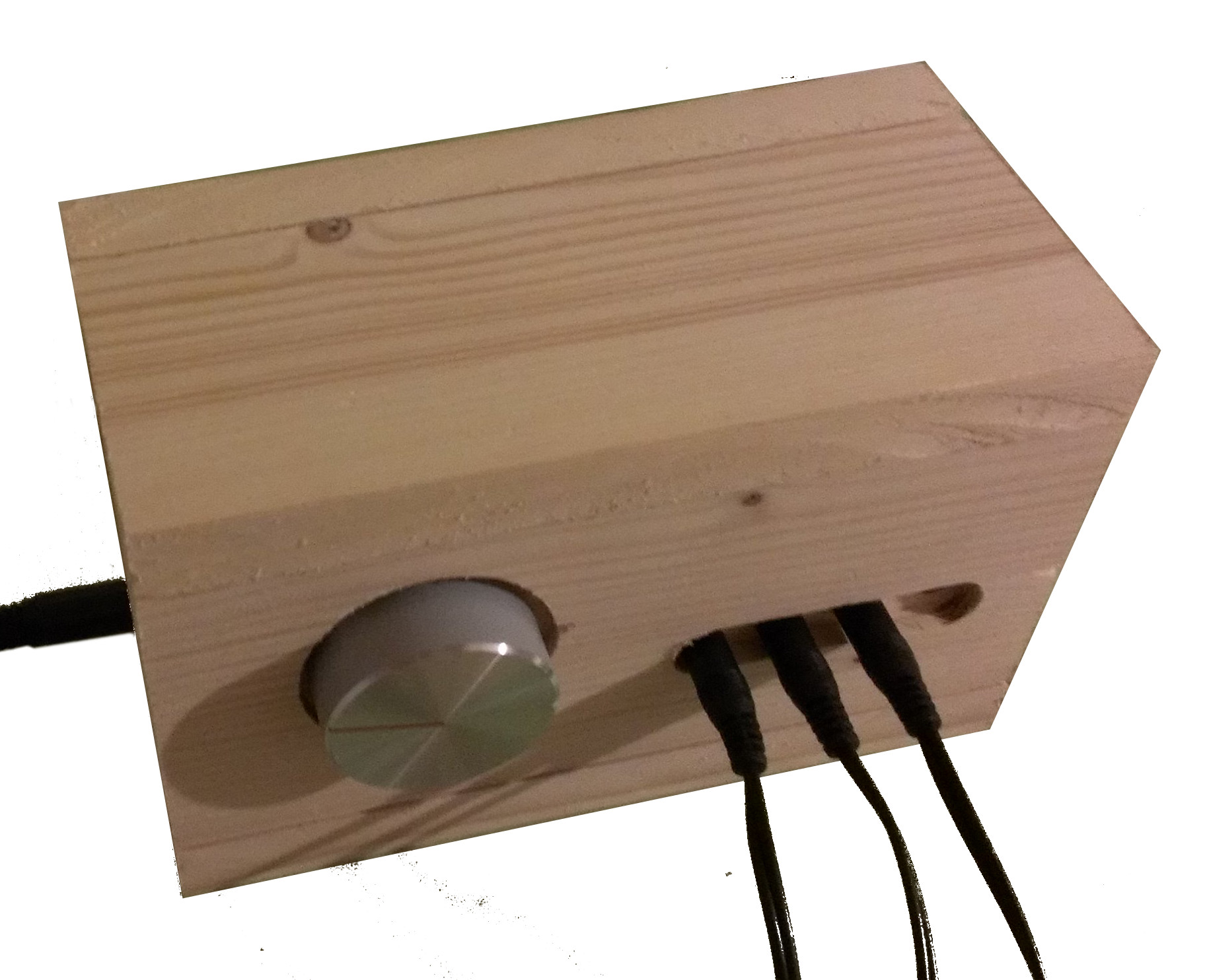
That odd location....
Forced us to make a box that was somewhat larger than expected. Certainly if you use 1.8cm thick wood to make a box.
|
Bibliography
| 1. | 3 Channel audio splitter |
| 2. | An audio circuit collection, part 1 Bruce Carter Texas Instruments Incorporated. Analog Applications Journal. November 2000. Analog and Mixed-Signal Products http://www.ti.com/lit/an/slyt155/slyt155.pdf |
| 3. | Avoid Common Problems When Designing Amplifier Circuits Charles Kitchen Analogue Dialogue. Volume 41. August 2007 http://www.analog.com/library/analogDialogue/archives/41-08/amplifier_circuits.html |
| 4. | Op-Amp Circuits; 14-10-2015 Ruye Wang http://fourier.eng.hmc.edu/e84/lectures/opamp/node3.html |
| 5. | NE5532x, SA5532x Dual Low-Noise Operational Amplifiers |
| 6. | Platinen selber ätzen |
| http://werner.yellowcouch.org/ werner@yellowcouch.org |  |